

Analysis: Increasing the computational power of microchips means using a process rooted in an early version of film photography
Computer chips have arguably been one of the key drivers for human progress over the past half century. As the impetus behind the technologies and devices that power our daily lives, the significance of advancing semiconductor technology cannot be overstated.
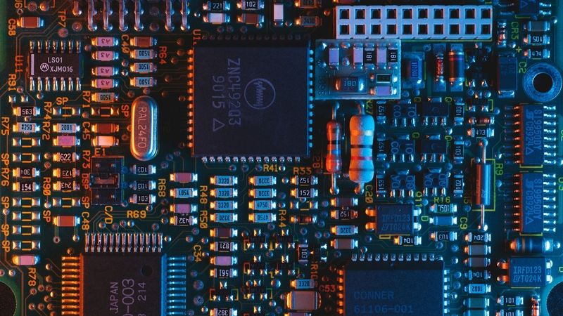
To improve the computational power of microchips, the number of transistors they contain must be increased. In 1965, Gordon Moore calculated that this number would double annually, a prediction that became known as Moore's Law.
This relentless pursuit of concentrating more transistors into the same volume of silicon enables the creation of smaller, more powerful and energy-efficient electronic components. Our reliance on technology is increasing with new requirements in big and complex data processing, artificial intelligence and machine learning. The ability to produce chips with unprecedented transistor densities is central to meeting these growing demands.
We need your consent to load this rte-player contentWe use rte-player to manage extra content that can set cookies on your device and collect data about your activity. Please review their details and accept them to load the content.Manage Preferences
From RTÉ Radio 1's The Business, editor of Silicon Republic Elaine Burke digs into the data around computer chips
To fabricate them, companies employ a process that has its roots in a 19th century invention, when William Henry Fox Talbot developed what he called "photogenic drawings", an early version of the film photography that preceded modern digital cameras. His use of papers coated with silver salts, which darkened when exposed to sunlight, was one of the first methods used to capture real images.
From there, a direct path can be traced through time to photolithography, the method used to draw patterns on the silicon when manufacturing chips today. The basic steps are still very similar to film-based photography, and many companies work in both fields, such as Nikon and Canon.
In photography, the film is coated with an emulsion which contains silver halide crystals embedded in gelatine. These react when exposed to light, darkening the emulsion and forming the latent image. The development step brings the image into sharp relief and the film is subsequently fixed to prevent blurring.
The economic importance of semiconductor manufacturing to Ireland cannot be overstated
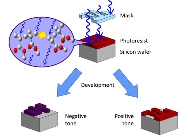
The steps are very similar in photolithography. The film is replaced by a silicon wafer, which is coated with a thin film of light sensitive material: the photoresist. The wafers are provided in the form of thin discs, typically 30 cm in diameter. Each wafer will produce 300 to 500 chips following processing.
Like the emulsion referred to earlier, the photoresist is responsible for the chemistry that occurs during exposure. Light is projected through a mask, creating a shadow pattern on the wafer. The exposed regions undergo chemical reactions depending on the type of photoresist used. In positive tone resists, the exposed regions become more soluble while in negative tone resists, they become less soluble.
The wafer is then washed with a solvent, dissolving the more soluble regions of the resist. This is equivalent to the development step in traditional film photography. The wafer is often baked to harden the photoresist on the silicon surface. It now has a pattern of protective photoresist and exposed silicon, and it is ready for the subsequent processing steps. These can include etching channels in the exposed silicon, filling the gaps with a metal or embedding different materials in the silicon itself, so that diodes and transistors can be formed.
Photolithography can be thought of as a type of printing process whose resolution will determine how small the features, like transistors, can be fabricated on a chip. This is largely determined by the wavelength of light used – a shorter wavelength allows you to print, and hence produce, smaller features.
Industry has used several clever tricks to push the lower limit for feature sizes down to tens of nanometres (1 nm = 1 billionth of a metre). The current technology uses deep ultraviolet light (a wavelength of 193 nanometres). However, 193 nm lithography has reached its physical limit and is not able to meet the next node of sub-10 nm feature sizes. Industry is switching to extreme ultraviolet (EUV) light, with a wavelength of 13.5 nm.
This presents an enormous challenge, as the old photoresists are not as effective with light of this wavelength. It is not yet fully clear if newly proposed materials will meet the exacting standards required to continue the drive to high-volume manufacturing of chips with feature sizes less than 5 nm, approximately the same size as a single haemoglobin molecule.
We need your consent to load this rte-player contentWe use rte-player to manage extra content that can set cookies on your device and collect data about your activity. Please review their details and accept them to load the content.Manage Preferences
From RTÉ Radio 1's Morning Ireland in March 2021, RTÉ Business Editor Will Goodbody on Intel's announcement of 1,600 new jobs at its Leixlip campus
Candidate resists must maintain the ultra-high resolution needed to replicate such small features. Moreover, they need sufficient sensitivity to undergo solubility changes with minimal EUV light doses, with enough strength to protect the silicon during further processing steps. This is the focus of our ultrafast investigations at DCU's NRF Femto lab.
The economic importance of semiconductor manufacturing to Ireland cannot be overstated. For example, a 2022 report from PWC calculates that Intel Ireland contributes almost €3bn annually to the Irish economy. Intel recently completed FAB 34, a €17bn investment at the Leixlip site that will use the new Intel 4 EUV process technology to produce high-end chips for the technology revolutions expected to dominate the next decade.
The incredible pace of miniaturisation has pushed semiconductor manufacturing almost to fundamental quantum limits
The unrelenting development of increasingly powerful computer chips will underpin the Irish and global tech sectors for decades to come. Ever greater computational performance is needed to power new and emerging fields such as AI and machine learning, self-driving cars, and the internet of things.
As demand for more powerful computers grows, semiconductor manufacturing companies throughout the world, like Intel, TSMC, Samsung and others will race to meet it. The incredible pace of miniaturisation has pushed semiconductor manufacturing almost to fundamental quantum limits. The next generation of chips will require further developments in EUV lithography to continue Moore's Law.
Follow the RTÉ Brainstorm WhatsApp channel for more stories and updates
The views expressed here are those of the author and do not represent or reflect the views of RTÉ